Showing posts with label Tutorial. Show all posts

Sunday, January 24, 2016

Operational Amplifiers


Why Are Operational Amplifiers Widely Used?
        This lesson is the first lesson on operational amplifiers, or op-amps as they are often called.
        Operational amplifiers are widely used in signal processing circuits, control circuits, and instrumentation.  Of all analog integrated circuits, the operational amplifier is the analog integrated circuit which has the most sales and is the most widely used in the widest variety of electronic circuits.  If you are an electrical engineer, you will probably encounter more operational amplifiers than any other integrated circuit device.  It's an important component for electrical engineers who design circuits using them and to all other kinds of engineers who use measurement and control circuits that contain operational amplifiers.

Where do you find Op-Amps?         Operational amplifiers are used in many places including:

Wednesday, January 20, 2016

IC Voltage Regulators

Image titled Make a Small Heater Step 1A voltage regulator is one of the most widely used electronic circuitry in any device. A regulated voltage (without fluctuations & noise levels) is very important for the smooth functioning of many digital electronic devices. A common case is with micro controllers, where a smooth regulated input voltage must be supplied for the micro controller to function smoothly.
You may also like this article on Regulated Power Supply
Voltage regulators are of different types. In this article, our interest is only with IC based voltage regulator. An example of IC based voltage regulator available in market is the popular 7805 IC which regulates the output voltage at 5 volts. Now lets come to the basic definition of an IC voltage regulator. It is an integrated circuit whose basic purpose is to regulate the unregulated input voltage (definitely over a predefined range) and provide with a constant, regulated output voltage.
An IC based voltage regulator can be classified in different ways. A common type of classification is 3 terminal voltage regulator and 5 or multi terminal voltage regulator. Another popular way of classifying IC voltage regulators is by identifying them as linear voltage regulator & switching voltage regulator.  There is a third set of classification as 1) Fixed voltage regulators (positive & negative) 2) Adjustable voltage regulators (positive & negative) and finally 3) Switching regulators. In the third classification, fixed & adjustable regulators are basically versions of linear voltage regulators. 

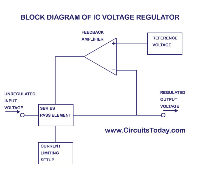
Block Diagram of 3 Terminal IC based Voltage Regulator

We have given below the block diagram of a 3 terminal IC based voltage regulator.
IC Voltage Regulator Block Diagram

PN Junction Diode and its characteristics

In chapter 1Understanding the PN junction , we have seen how a PN junction is formed from a p-type and n-type semiconductor. We have also learned about diffusion current, depletion region, drift current and barrier potential. If you find these terms foreign, just read the chapter about “understanding the pn junction” once more. Lets just make some questions. What is the use of a PN junction? Why have scientists created a pn junction device? What kind of problem it solves ? Learning anything is really fun when we question it. So these are our questions. Why there exists a pn junction in this world! ?;)
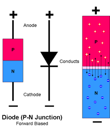
To get an answer to all these questions, lets first try to understand the characteristics of a PN junction. We know a pn junction has a “barrier potential”. Only if we overcome this “barrier potential” by applying an external voltage to the pn junction, we would be able to make it conducting. This simply means, current will pass through the pn junction only if we apply an external voltage higher than the “barrier potential” of pn junction. In chapter 1, we have seen that  net current inside a pn junction is zero. Inorder to understand the behavior of a pn junction we need to make it conducting by applying an external voltage over a range (say from 0 volts 5 or 10 volts ), and then we study how the current passed through the pn junction varies with increasing voltage levels. To apply an external voltage, we usually connect 2 metallic contacts at the two ends of the pn junction (known as terminals); one on the p-side and other on the n-side. A PN junction with two metallic contacts is known as a pn junction diode or a semiconductor diode. 
Note:- I have written an interesting article which tells the story behind invention & discovery of PN Junction diode. If you like to read the story, follow here:- Story behind Invention & Discovery of PN Junction

Understanding the PN Junction

Whenever someone decides to learn electronics, the first question that comes to his mind may be – “Where shall I begin?“. I would say, one shall begin at a junction the “pn junction“. We know semiconductor devices like transistors and diodes are the basic building units of any equipment that involves electronics, say tablet computers to the sophisticated MRI machines! How these basic units like transistors and diodes are formed ? or how are they made ? The answer lies in understanding “PN Junction”. A PN junction is the basic building block of many semiconductor devices like diodes and transistors.
Note:- I have written an interesting article which tells the story behind invention & discovery of PN Junction diode. If you like to read the story, follow here:- Story behind Invention & Discovery of PN Junction

How a PN Junction is formed?

Pulse Width Modulation – What is it?

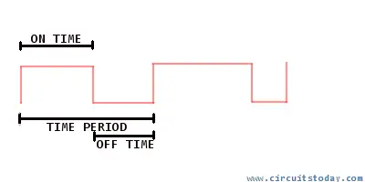
The good definition of Pulse Width Modulation (PWM) is in the name itself. It means modulating/varying the width of the pulse (Not the frequency). To best understand what PWM is, let us first see some basic terminologies.
Microcontrollers are intelligent digital components which live on binary signals. Best representation of a binary signal is a square wave. The following diagram explains the basic terminologies associated with a square wave signal.


Higher Order Filters

Higher Order Filters

From the discussion made so far on the filters, it may be concluded that in the stopband the gain of the filter changes at the rate of 20 db/decade for first-order filters and 40 db/decade for second-order filters. This means that as the order of the filter is increased, the actual stopband response of the filter approaches its ideal stopband characteristics. In general, a third-order filter produces 60 db/decade, a fourth-order filter produces 80 db/decade and so on.
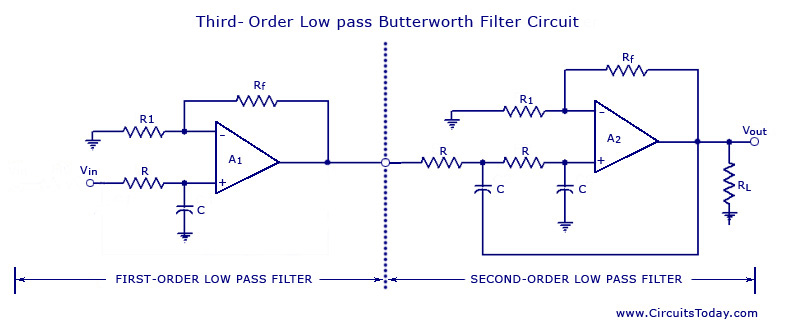
Higher-order filters, such as third, fourth, fifth, and so on, are built simply by using the first and second-order filters.
The simplest way to build a third-order low-pass filter is by cascading a first order filter with a second-order. Similarly a fourth-order low-pass filter can be formed by cascading two second-order low-pass filters. Although there is no limit to the order of the filter that can be formed, as the order of the filter increases, so does its size. Also the accuracy declines, in that the difference between the actual stopband response and the theoretical stopband re­sponse increases with an increase in the order of the filter.

All pass filters

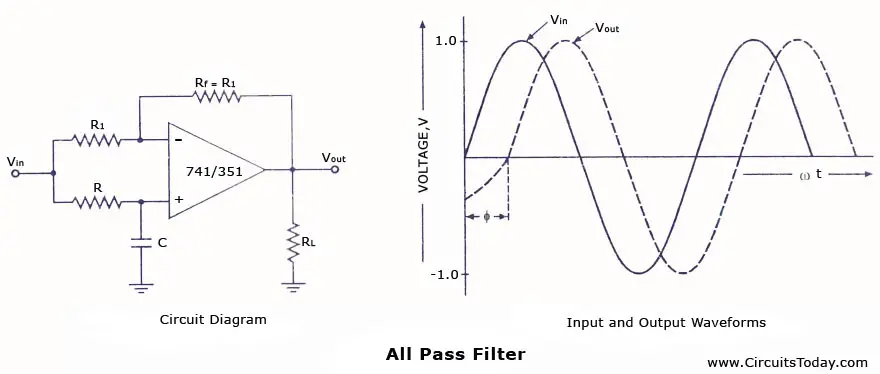
An all-pass filter is that which passes all frequency components of the input signal without attenuation but provides predictable phase shifts for different frequencies of the input signals. The all-pass filters are also called delay equalizers or phase correctors. An all-pass filter with the output lagging behind the input is illustrated in figure.
All pass filter circuit and frequency response

Active and Passive filters

Active and Passive filters – A Comparison:

The simplest approach to building a filter is with passive components (resistors, capacitors, and inductors). In the R-F range it works quite well but with the lower frequencies, inductors create problems. AF inductors are physically larger and heavier, and therefore expensive. For lower frequencies the inductance is to be increased which needs more turns of wire. It adds to the series resistance which degrades the inductor’s performance.
Input and output impedances of passive filters are both a problem, especially below RF. The input impedance is low, that loads the source, and it varies with the frequency. The output impedance is usually relatively high, which restricts the load impedance that the passive filter can drive. There is no isolation between the load impedance and the passive filter. Thus the load will have to be considered as a component of the filter and will have to be taken into consideration while determining filter response or design. Any change in load impedance may significantly alter one or more of the filter response characteristics.

X-Ray Lithography

The photolithography has its resolution limited by diffraction effects. To improve the resolution, therefore, the diffraction effects are reduced by reducing the wavelength. However, if the wavelength is reduced further, all optical materials become opaque because of the fundamental absorption, but transmission increases again in the X-ray region. This led to the requirement of X-rays for lithography purpose.
In X-ray lithography an X-ray source illuminates a mask, which casts shadows on to a resist-covered wafer. The mask and resist material for X-ray lithography are mainly determined by the absorption spectra of these materials in the X-ray region.

Photonic Integrated Circuit

Photonic Integrated Circuit Technology

Photonic Integrated Circuit (also known as PIC), is a complex integrated circuit which incorporates a lot of optical devices to form a single photonic circuit. The main difference between a PIC and an Electronic IC is that PIC is analogous to an Electronic Integrated Circuit.  Many optical devices like optical amplifiers, multiplexers, de-multiplexers, optical lasers, attenuators and also detectors are integrated on to a Photonic Integrated Circuit. For a large-scale operation of such a device thousands of optical devices will be integrated on to the device.
In a PIC, the signals are sent by superimposing them on wavelengths usually in the range between the visible spectrum and infrared. The range usually is between 800 nanometers and 1700 nanometers.
In 2005, during a development of a laser light through silicon in an electronic integrated circuit, there occurred a problem with quantum noise, which prevented the generation. This problem was easily overcome by a photonic integrated circuit, which easily created the laser light and that too in a higher bandwidth, within the circuit as a single medium. Thus the importance of PIC was known.

Photolithographic

When a sample of crystalline silicon is covered with silicon dioxide, the oxide-layer acts as a barrier to the diffusion of impurities, so that impurities separated from the surface of the silicon by a layer of oxide do not diffuse into the silicon during high-temperature processing. A p-n junction can thus be formed in a selected location on the sample by first covering the sample with a layer of oxide [oxidation step] removing the oxide in the selected region, and then performing a predeposition and diffusion step. The selective removal of the oxide in the desired area is performed with photolithography. Thus, the areas over which diffusions are effective are defined by the oxide layer with windows cut in it, through which diffusion can take place. The windows are produced by the photolithographic process. This process is the means by which microscopically small electronic circuits and devices can be produced on silicon wafers resulting in as many as 10000 transistors on a 1 cm x 1 cm chip.
In fact photolithography or optical lithography is a kind of lithography. The lithography technique was first used in the late 18th century by people interested in art.  A lithograph is a less expensive picture made from a flat, specially prepared stone or metal plate and the lithography is art of making lithographs. Therefore, lithography for IC manufacturing is analogous to the lithography of the art world. In this process the exposing radiation, such as ultraviolet (UV) light in case of photolithography, is transmitted through the clear parts of the mask. The circuit pattern of opaque chromium blocks some of die radiation. This type of chromium/glass mask is used with UV light. Other types of exposing radiations are electrons, X-rays, or ions. Thus for IC manufacturing we have following types of lithography. Photolithography has been explained in this post. To know about the other types of lithographic process, click on the link below.

Smart Antennas

What is a Smart Antenna?

Smart Antennas, also known as multiple antennas, adaptive array antennas, and so on is used to increase the efficiency in digital wireless communication systems. It works by taking the advantage of the diversity effect at the transceiver of the wireless system that is the source and the destination. The term diversity effect refers to the transmission and reception of multiple radio frequencies that are used to decrease the error during data communication and also to increase data speed between the source and the destination.
This type of technology has already found its significance in most of the wireless communication systems as special antenna arrays are used with signal processing algorithms which can easily locate and track the different wireless targets such as mobiles. It is also used to calculate the beam forming vectors and the direction of arrival [DOA] of the signal.

Difference between Conventional Antenna and Smart Antenna

The main difference is related with the way both the systems deal with the problems caused by multipath wave propagation.

Resistor Color Code Chart – Understanding Resistance Color Coding

“Color coding” is used in electronics to identify between different components. In the case of resistors, color coding is used to identify a specific resistance value, for example a 100 ohms resistor or a 1 kilo ohms resistor with 5% tolerance. Electronic components like resistors are very small in size and its difficult to print its value directly on to the component surface. Hence a standard was formed in 1920 by then Radio Manufacturers Association (now part of EIA – Electronic Industries Alliance) to identify values and ratings of electronic components by printing color codes on them.  Color coding technique makes it easy to print values (based on color codes) on small components, such as resistors and facilitates  cost effective manufacturing.
This technique of “color coding” has 2 disadvantages. The first one appeals to general users where it becomes difficult to distinguish between colors (for example “Red” and “Brown” ) when the component is over heated. But this is not a major concern as the exact value can be easily identified using a multimeter (in case of confusion). The next drawback is for a specific group of people – color blind people can not identify the device using color codes. However they too can depend on multimeter to identify resistance values.

How to Identify Resistor Color Code

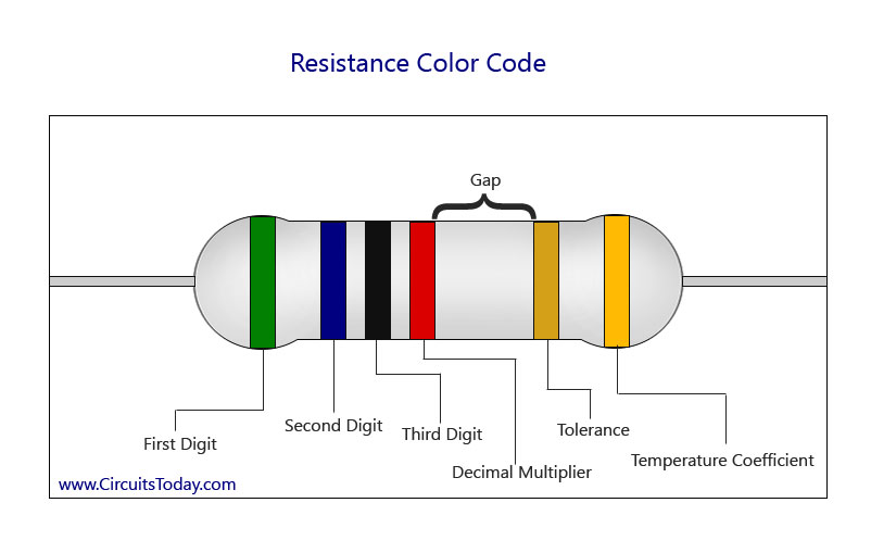
The figure below shows the layout of the bands, the multiplier and the tolerance value of a resistor. For a 6-band resistor, an additional temperature coefficient band is provided.

The gap between the multiplier and the tolerance specifies the left and right side of the resistor.  So here are the key points;
4 band resistor – has 3 color bands on left side and one color band on right side. First two bands represent significant digits, the 3rd band represents multiplier and the fourth band on right side represents tolerance.

Push pull amplifier

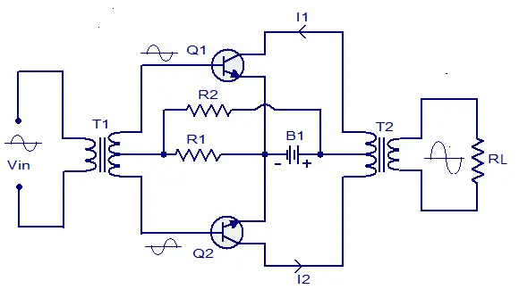
A push pull amplifier is an amplifier which has an output stage that can drive a current in either direction through through the load. The output stage of a typical push pull amplifier consists of of two identical BJTs or MOSFETs one sourcing current through the load while the other one sinking the current from the load. Push pull amplifiers are superior over single ended amplifiers (using a single transistor at the output for driving the load) in terms of distortion and performance. A single ended amplifier, how well it may be designed will surely introduce some distortion due to the non linearity of its dynamic transfer characteristics. Push pull amplifiers are commonly used in situations where low distortion, high efficiency and high output power are required. The basic operation of a push pull amplifier is as follows: The signal to be amplified is first split into two identical signals 180° out of phase. Generally this splitting is done using an input coupling transformer. The input coupling transformer is so arranged that one signal in applied to the input of one transistor and the other signal is applied to the input of the other transistor. Advantages of push pull amplifier are low distortion, absence of magnetic saturation in the coupling transformer core, and cancellation of power supply ripples which results in the absence of hum while the disadvantages are  the need of two identical transistors and the  requirement of bulky and costly coupling transformers.

Class A push pull amplifier.

pushpull amplifier

MOS – Controlled Thyristor (MCT)

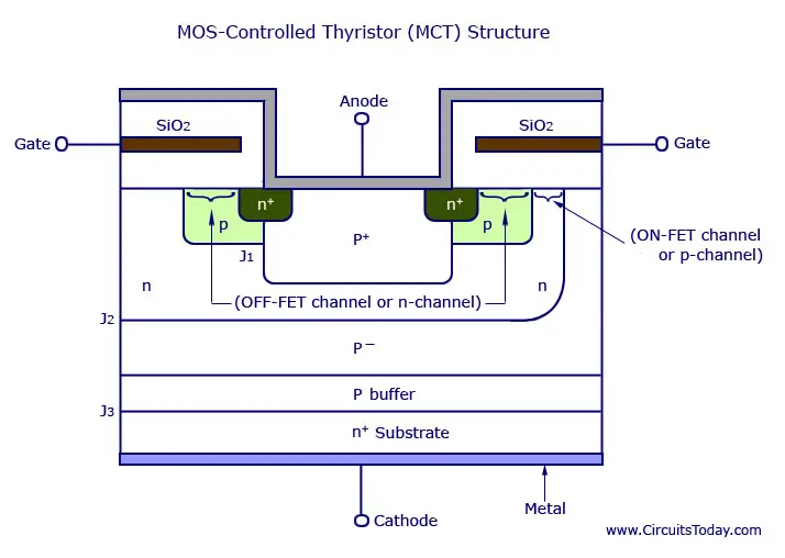
Out of many semiconductor controlled devices, MCT is considered to be the latest. The device is basically a thyristor with two MOSFET’s built into the gate structure. A MOSFET is used for turning ON the MCT and another one is used for turning it OFF. The device is mostly used for switching applications and has other characteristics like high frequency, high power, and low conduction drop and so on. An MCT combines the feature of both conventional four layer thyristor having regenerative action and MOS- gate structure. In this device, all the gate signals are applied with respect to anode, which is kept as the reference. In a normally used SCR, cathode is kept as the reference terminal for gate signals.
The basic structure of an MCT cell is shown in the figure below.
MOS Controlled Thyristor (MCT) Structure

Transformer

Most of the electronic circuits used in Circuitstoday.com have different applications of the transformer. Therefore, it is important to know the working principle, construction and types of transformers used in different analog circuits.

Transformer – Working Principle

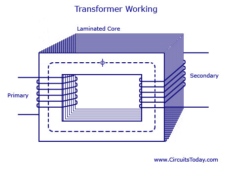
A transformer can be defined as a static device which helps in the transformation of electric power in one circuit to electric power of the same frequency in another circuit. The voltage can be raised or lowered in a circuit, but with a proportional increase or decrease in the current ratings.
The main principle of operation of a transformer is mutual inductance between two circuits which is linked by a common magnetic flux. A basic transformer consists of two coils that are electrically separate and inductive, but are magnetically linked through a path of reluctance. The working principle of the transformer can be understood from the figure below.
Transformer Working
Transformer Working

Introduction to uA 741 Op-Amp

About the uA741 Op-amp IC

The 741 IC was designed by Dave Fullagar of Fairchild Semiconductor in 1968. The 741 IC is the successful predecessor of the LM 101 IC, and the only difference between the two was that an additional 30pF internal compensation capacitor was added for the 741 IC. But, this simple addition has made this IC evergreen in the electronics world and is still manufactured by different companies in different versions and specifications, and is made recognizable by adding the famous number 741 in the series.
The 741 IC is developed using the planar epitaxial process (Refer:- Epitaxial Devices – Characteristics). The IC is made ideal for use as integrator, summing amplifier, voltage follower and other basic applications.
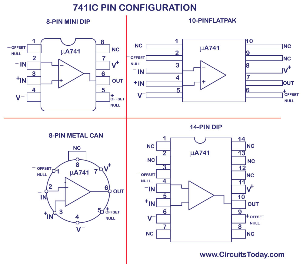
The 741 IC is available in the market as 8-pin metal can, 10-pin flat pack, 8 or 14 pin DIP. The pin configuration for thse packages are shown below.
Image titled Make a Small Heater Step 1uA741 IC Pin Configuration
uA741 IC Pin Configuration

Thursday, January 14, 2016

Light Emitting Diode How it Works?

LEDs form an inevitable part in the modern electronics as simple indicators to optical communication devices. Light Emitting Diodes exploit the property of the p-n junction to emit photons when it is forward biased. LEDs are specially made diodes to emit light when a potential is applied to its anode and cathode.

The history of LED date backs to 1907 when Captain Henry Joseph observed the property of electro-luminescence in Silicon Carbide. The first LED was designed in 1962. It was developed by Holonyak worked at General Electric (GE). It was a GaAsP device. The first commercial version of LED came in the market during 1960s.
LED technology industry became a boom during 1970s with the introduction of Gallium Aluminium Arsenide (GaAlAs). These LEDs are high bright types and are many times brighter than the old diffused types. Blue and White LEDs was introduced in 1990 which uses Indium Gallium Nitride (InGaN) as the semiconductor. White LED contains a blue chip with white inorganic Phosphor. When blue light strikes the phosphor, it emits white light.

What makes LED ideal?

LEDs are extensively used in electronic circuits because of its advantages over bulbs. Some important features that make LED ideal in electronic circuits are:
  • LEDs are encapsulated in plastic or resin cases so that they can withstand mechanical shocks.
  • Unlike bulbs, LEDs do not generate heat and power loss through heating is practically nil.
  • LEDs require very low current and voltage typically 20 milliampere current and 1.8 volts. So these are ideal in battery operated circuits.

What is inside an LED?

Inside the casing of an LED, there are two terminal posts connected by a small chip made of Gallium compound. This material exhibits the property of photon emission when the p-n junction is forward biased. Different colours are produced by dopping the base material with other substances.
Inside the Light Emitting Diode

Tuesday, November 10, 2015

INCREASING THE INPUT IMPEDANCE

The input impedance of a low cost analogue multimeter can be improved using this circuit. The approximate impedance increase will be about 250. 
The LED provides a fixed reference voltage for zero setting of the multimeter via VR1.

CONSTANT CURRENT SOURCE

In the following circuit an LED is used to give a fixed reference voltage to a transistor. The output constant current I out is given by:
The LED lights up only when a load is connected at the output. Thus it indicates when the circuit is operating.


The operation of the circuit can be made clearer by re-arranging the components as follows:


The output will be limited to 100mA by using a red LED and 10R for Re.
The output will be limited to 500mA by using a red LED and 2R2 for Re.
The output will be limited to 1A by using a red LED and 1R0 for Re.

Arduino Based Auto Transport Device

AUTO TRANSPORT DEVICE is idea of making a self-driving device that is low cost and can carry high load to its destination. This device is ...