Showing posts with label Op amp. Show all posts

Sunday, January 24, 2016

Operational Amplifiers


Why Are Operational Amplifiers Widely Used?
        This lesson is the first lesson on operational amplifiers, or op-amps as they are often called.
        Operational amplifiers are widely used in signal processing circuits, control circuits, and instrumentation.  Of all analog integrated circuits, the operational amplifier is the analog integrated circuit which has the most sales and is the most widely used in the widest variety of electronic circuits.  If you are an electrical engineer, you will probably encounter more operational amplifiers than any other integrated circuit device.  It's an important component for electrical engineers who design circuits using them and to all other kinds of engineers who use measurement and control circuits that contain operational amplifiers.

Where do you find Op-Amps?         Operational amplifiers are used in many places including:

Wednesday, January 20, 2016

Introduction to uA 741 Op-Amp

About the uA741 Op-amp IC

The 741 IC was designed by Dave Fullagar of Fairchild Semiconductor in 1968. The 741 IC is the successful predecessor of the LM 101 IC, and the only difference between the two was that an additional 30pF internal compensation capacitor was added for the 741 IC. But, this simple addition has made this IC evergreen in the electronics world and is still manufactured by different companies in different versions and specifications, and is made recognizable by adding the famous number 741 in the series.
The 741 IC is developed using the planar epitaxial process (Refer:- Epitaxial Devices – Characteristics). The IC is made ideal for use as integrator, summing amplifier, voltage follower and other basic applications.
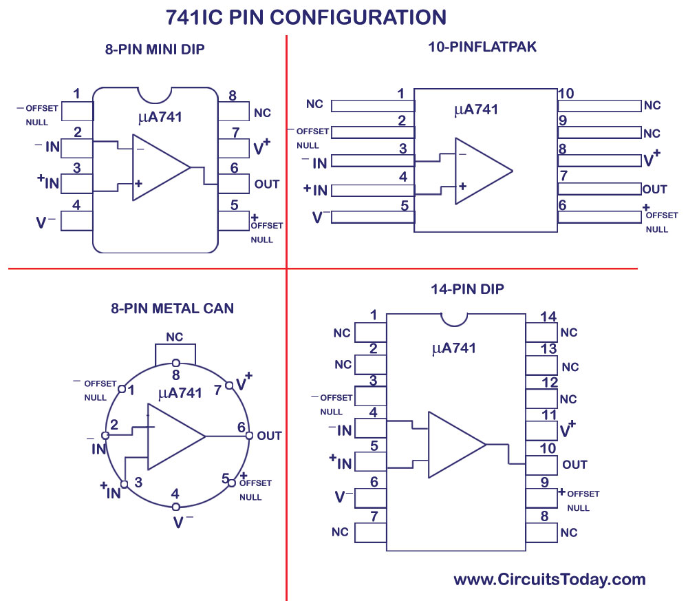
The 741 IC is available in the market as 8-pin metal can, 10-pin flat pack, 8 or 14 pin DIP. The pin configuration for thse packages are shown below.
Image titled Make a Small Heater Step 1uA741 IC Pin Configuration
uA741 IC Pin Configuration

Sunday, November 08, 2015

DIY Operational Amplifier

While this op amp may actually have some utility, it is intended mainly as an educational exercise. I guarantee that if you build and experiment with this circuit, you will learn and appreciate what is inside monolithic versions of the same. There is so much to learn and know about op amps that one hardly knows where to start – I suggest that this is a good place to start. Applications include inverting amplifier, non-inverting amplifier, integrator and voltage comparator. One practical application may be a headphone amplifier. This is intended to be basic rather than exhaustive.

DIY Op Amp Schematic

DIY Operational Amplifier Schematic

Op Amp Application

Op Amp Application
Power supplies
The recommended power source is a split power supply (±6 to ±15V). Dispelling one common misconception, note that the ± power supplies need not be equal in voltage. If unequal, the maximum output voltage swings cannot be equal in both polarities.
With appropriate biasing and capacitor coupling techniques, it may also be used with a single supply, but this aspect is not discussed here.
Input differential pair
Q1 & Q2 make up a differential amplifier – the differential amplifier is the foundation of the op amp, offering both inverting and non-inverting inputs so it may be used in a myriad of applications. Using matched transistors, the input voltages are closely matched – this is called the input offset voltage. For reference, recall that a single transistor amplifier has an input voltage of about 650mV. However, in a differential amplifier, the 650mV offsets balance each other so that the difference is generally below 10mV.
Another important parameter is input bias current – it is always the object to keep this as low as possible – in this circuit, it runs at about 100nA. Ideally, the input bias currents are equal, but if not the difference is referred to as input offset current. Generally this parameter is disregarded except in high impedance or very high accuracy circuits.
Biasing the differential amplifier
A differential amplifier requires a current source – this may be either a fixed resistor to a negative supply or a current source as in this case. The fixed resistor is effective if the negative supply is always the same and/or if it is applied as an inverting amplifier where the input nodes are at zero volts. The current source accommodates variations in power supply voltage selection as well as a wide common-mode voltage range that is required for non-inverting amplifiers.
The current source consists of a voltage reference consisting of R1, D1 & D2. With the base of Q3 running at 1.2V, the emitter of Q3 operates at about 500mV off the negative rail. Since the voltage across R3 is now fixed and the collector current is essentially equal to the emitter current, the collector current is no longer a function of the input voltage. This is the basic operation of the current source.
The current source is split by the differential amplifier so that the collector currents of Q1 & Q2 are equal.
Adjusting the input offset voltage
A good place to start is by matching the Vbe and hFE characteristics of Q1 & Q2. Beyond this, the values of R2 & R3 are critical. Either of these may be adjusted to null input offset voltage – I varied R3.
Obtaining an output from the differential amplifier
R2 is sized so that its voltage drop is 650mV – the same as the Vbe threshold of Q4 that is configured as a common emitter transistor amplifier.
Increasing the gain and output voltage swing of Q4
Rather than the usual load resistor, the collector of Q4 operates into another current source (Q5). This offers the advantage of superior drive of the output transistors as the output voltage approaches the negative rail. It also increases the voltage gain of this stage significantly because a current source has a high dynamic resistance and voltage gain of a transistor is a function of the load resistance.
Output stage
Q6 & Q7 make up a complementary symmetry output stage. This is in effect a glorified emitter follower that operates in either the positive or negative polarities. The two transistor base terminals are biased via two silicon diodes. Since the diodes limit the base voltage to a point just below the transistor Vbe threshold, there is no quiescent output stage current. This is also called a zero bias configuration because both transistors are normally off. The drawback is that it is subject to potential crossover distortion – I could not detect any. Crossover distortion occurs when the output current switches from the top transistor to the bottom transistor. Some monolithic (IC) op amps like the LM358 and LM324 have the same problem. Other op amps solve this problem by adding a resistor in series with the two bias diodes – this also requires emitter resistance which tends to complicate the circuit. Crossover distortion is most apparent at low signal levels where the op amp spends all its time switching transistors.
Frequency compensation
C1 provides frequency compensation in order to reduce the gain at high frequencies where it may be subject to oscillation (instability). Without compensation, mine oscillated at 2mHZ.
Shortcomings
While there are no perfect op amps, some monolithic devices are very, very good. This circuit has some real shortcomings as follows:
  • No provision for thermal stability – operate at room temperature only
  • Relatively high input offset voltage, but can be nulled
  • Lack of output overcurrent protection
  • Limited open loop voltage gain – the open loop voltage gain of a monolithic device is at least an order of magnitude higher.
  • Potentially high crossover distortion
Suggested exercises for the experimenter
  • Measure quiescent power supply current – very easy
  • Null input offset voltage – set up with a voltage gain of 100, ground input and adjust R2 or R3 so that the output voltage is zero
  • Observe thermal stability – after the input offset voltage has been nulled, blow hot air on the circuit and watch the output voltage shift (use hair dryer)
  • Measure input bias current – add 100K resistor in series with input terminals, measure voltage drop across resistor, then calculate current
  • Plot frequency response at 1VAC output and at full output voltage
  • Measure open loop gain – set up as an inverting amplifier – with full output voltage, measure input node voltage – divide AC output voltage by AC input node voltage (note, this cannot be done with a monolithic op amp due to itsextremely high open loop gain).
  • Determine maximum slew rate in both polarities (positive going and negative going)
  • Using oscilloscope, see how well it amplifies a sine wave.
  • Perhaps you can experiment upon and improve upon this relatively crude circuit
Oscillographs
Sine Wave Output
Photos 
Conclusions
I hope you learned from this exercise – now we all can better appreciate the bargain and power of monolithic op amp integrated circuits that come not only as singles, but duals and quads

What is the difference between op amps and comparators?

While both operational amplifiers and voltage comparators have been with us since before 1970, the similarities and differences tend to be vague. This discussion will help in understanding this important issue.
I well remember the first time that I saw an operational amplifier; it was 1965 at Cambridge Electron Accelerator –it was a mysterious box containing numerous transistors that could be connected in various ways for various functions. Both analog and digital integrated circuits (RTL –Resistor Transistor Logic) would soon be introduced, but I never could have guessed what the future would hold. Now some 50years later having used both op amps and comparators, I have good understanding of these devices and wish to pass some practical information along.
Popular devices
Perhaps the most popular operational amplifiers are the venerable LM741 and the more recent LM324. The most popular comparators include the LM311 and the LM339. These were developed by National Semiconductor, soon became industry standards and subsequently licensed and enhanced by numerous manufacturers including TI, Motorola etc.
Schematics
Guts of the LM339 & LM324
A cursory glance may suggest that the two schematics are very similar with both having identical differential inputs, but observe the differences in the output structure. The LM324 has a complementary output while the LM339 is open collector. In the complementary output, current can flow in either direction as required (either source or sink) while the open collector output can only sink current. This basic difference is typical of all op amps and comparators (although a few comparators have complementary outputs).
Another more subtle difference is the presence of a compensation capacitor in the op amp –this is typical of perhaps 99% of all op amps. An operational amplifier is slowed down by the compensation capacitor in order to make it stable (prevent oscillation), while a comparator is intended to be as fast as possible in order to minimize propagation delay and to provide fast transition time at the output. However, both op amps and comparators often share this common problem: unwanted oscillation.
Application issues
The operational amplifier is intended for linear operation where the output may be at any voltage within the limits of the power supply rails. The voltage comparator is simply a 1bit analog to digital converter where the output is always in positive or negative saturation.
Power supplies (or rails)
The ground rail is generally logic common. In a single supply comparator, it is also generally the negative rail or the most negative voltage in the circuit. Some comparators like the LM311 cannot compare voltages at ground potential due to limitations in the common mode input voltage range so they require a negative rail to power the analog section. These devices offer a separate logic ground pin that is tied to logic common. So in the LM311 class of comparators there are (3) rails: common, analog positive and analog negative. A possible 4th rail would be the logic positive rail that is equal or lower in voltage than the analog positive power supply rail –this is what powers the output pull-up resistor. The analog positive and negative rails are often ±12V, but can actually be whatever is desired or required such as ±5V –also, they need not be equal in voltage.
Note that some comparators (perhaps 10%) have a complementary rather than open collector output –with such, the analog positive rail must be equal in voltage to the logic positive rail.
Open collector output
The open collector output is the usual means of interfacing the comparator output to the logic input. Such requires an external pull-up resistor. It allows the logic positive rail to be lower in voltage than the analog positive rail. Open collector outputs also provide the means of a “wired OR” connection where multiple open collector outputs are tied together –all open collector outputs must be high (OFF) in order for the output to go high.
ORing the Outputs
Op amps as comparators
Op amps are frequently used as comparators –I do this commonly. This is practical where high speed is not a requirement and where single supply operation is feasible. Note also that op amps and comparators have incompatible pin-outs and cannot easily be substituted.
Comparators as op amps
Very, very seldom are comparators used as op amps, but never say never. Here is an application note that shows how to make it work. The addition of the output capacitor slows the device so that it can operate without oscillation in the linear output voltage range. The only time this might be practical is when a low performance op amp function is required, but the only device available is one section of an LM339 quad comparator. Now, I have never done this, but it would make a great experiment.
LM339 as an Op Amp
Use the LP311 instead of the LM311
While the LM311 will probably never go away, it is a power hog with a supply current of 5mA. The LP311 runs about 300uA –much better for battery and experimental applications. “LP” indicates “Low Power.”
Datasheets

Test Op Amps Via Simple Input Offset Voltage Measurement

Measuring this one vital parameter (Input Offset Voltage) provides a simple means of determining if the DUT (Device Under Test) is either good or bad. The circuit is very simple, requiring only four garden variety components and selector switch (or protoboard) to accommodate devices with multiple sections.
Schematic
Input Offset Voltage Test Schematic
Voltage follower connection
Each of the op amps to be tested is wired as a voltage follower (output connected to the inverting input). Virtually all garden variety op amps are stable in the voltage follower connection. The gain is unity (or 1) so that the voltage at the output is supposed to be exactly the same as the voltage on the non-inverting input. Any error reflects the input offset voltage, and can be easily measured with a good DVM.
DVM
My 15year old Radio Shack 22-174B DVM handles it well, reading only 0.1mV with the leads shorted (see photo) –ideally it should read zero mV –your DVM may do better or perhaps it even has 10uV resolution.
Input offset measurements with a random LM324 out of my junkbox
Pin 1: 0mV
Pin 7: 0.4mV
Pin 8: 1.2mV
Pin 14: 1mV
Specification: ±7mV max
My observation is that this is a good device with all sections measuring well below the ±7mV maximum.
Implications
For the input offset voltage to read within the limits, implies that both the op amp input and output circuit structures are working properly and have not been damaged via electrostatic discharge, or has not been fried by fault current etc.
Certainly, there are far more parameters that may be measured such as input bias current, input offset current, slew rate, output current limit, output saturation voltages (high & low), quiescent power supply current etc., but to measure all parameters would take all day unless one has an automated test fixture…and already has it programmed…
Conclusion
The input offset voltage measurement is a very good thermometer for determining device health.
Photos

Arduino Based Auto Transport Device

AUTO TRANSPORT DEVICE is idea of making a self-driving device that is low cost and can carry high load to its destination. This device is ...