The photolithography
has its resolution limited by diffraction effects. To improve the
resolution, therefore, the diffraction effects are reduced by reducing
the wavelength. However, if the wavelength is reduced further, all
optical materials become opaque because of the fundamental absorption,
but transmission increases again in the X-ray region. This led to the
requirement of X-rays for lithography purpose.
In X-ray lithography
an X-ray source illuminates a mask, which casts shadows on to a
resist-covered wafer. The mask and resist material for X-ray lithography
are mainly determined by the absorption spectra of these materials in
the X-ray region.
X-Ray Resist
An electron resist can
also be referred to as an X-ray resist, since an X-ray resist is
exposed largely by the photoelectrons produced during X-ray absorption.
The energies of these photoelectrons are much smaller than the 10 keV to
50 keV energies used in electron lithography, making proximity effects
negligible in the case of X-ray and promising higher ultimate
resolution.
Most of the polymer
resists containing only H, C, and 0, absorb very small X-ray flux. This
small absorption has the advantage of providing uniform exposure
throughout the resist thickness and the disadvantage of reduced
sensitivity. .
As in optical and
election lithography, the negative resists are limited in resolution by
swelling during development. Thus minimum features of only 0.75 micro
meters can be resolved in a commercial resist.
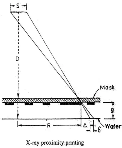
Proximity Printing
Since the wavelength
of X-ray is small, diffraction effects can be ignored and simple
geometrical considerations can be used in relating the image to the
pattern on the mask. The opaque parts of the mask cast shadows on to the
wafer below. The edge of the shadow is not absolutely sharp because of
the finite diameter of the focal spot of the electrons on the anode
[X-ray source] at a finite distance from the mask. The blurring of
shadow can be evaded by the following equation.
∂ = Sg/D
Where ∂ = blur
g = gap between mask and the wafer
D = Distance of source from the mask

X-Ray Lithography
X-Ray Sources
In earlier years of
development X-ray sources was often an electron beam evaporator with its
chamber modified to accept a mask and wafer. The target metal could be
changed easily to modify the X-ray spectrum. X-ray generation by
electron bombardment is a very inefficient process. Most of the input
power is converted into heat in the target. The X-ray flux is generally
limited by the heat dissipation in the target. Much high X-ray fluxes
are available from generators which have high speed targets. Another
type of source, which provides still greater amount of flux, is the
plasma discharge source in which the plasma is heated to a temperature
high enough to produce X-radiation. The plasma chamber has problems such
as reliability and contaminations.
X-Ray Masks
The mask for X-ray
lithography consists of an absorber on a transmissive membrane
substrate. The absorber is usually gold which is a heavy metal. Also it
can be easily patterned. The transmissive membrane substrate is a
polymer such as polymide and polyethylene terephthalate.


No comments:
Post a Comment