A push pull amplifier is an amplifier
which has an output stage that can drive a current in either direction
through through the load. The output stage of a typical push pull
amplifier consists of of two identical BJTs or MOSFETs one sourcing
current through the load while the other one sinking the current from
the load. Push pull amplifiers are superior over single ended amplifiers
(using a single transistor at the output for driving the load) in terms
of distortion and performance. A single ended amplifier, how well it
may be designed will surely introduce some distortion due to the non
linearity of its dynamic transfer characteristics. Push pull amplifiers
are commonly used in situations where low distortion, high efficiency
and high output power are required. The basic operation of a push pull
amplifier is as follows: The signal to be amplified is first split into
two identical signals 180° out of phase. Generally this splitting is
done using an input coupling transformer. The input coupling transformer
is so arranged that one signal in applied to the input of one
transistor and the other signal is applied to the input of the other
transistor. Advantages of push pull amplifier are low distortion,
absence of magnetic saturation in the coupling transformer core, and
cancellation of power supply ripples which results in the absence of hum
while the disadvantages are the need of two identical transistors and
the requirement of bulky and costly coupling transformers.
Class A push pull amplifier.
A push pull amplifier can be made in
Class A, Class B, Class AB or Class C configurations. The circuit
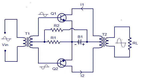
diagram of a typical Class A push pull amplifier is shown above. Q1 and
Q2 are two identical transistor and their emitter terminals are
connected together. R1 and R2 are meant for biasing the transistors.
Collector terminals of the two transistor are connected to the
respective ends of the primary of the output transformer T2. Power
supply is connected between the center tap of the T2 primary and the
emitter junction of the Q1 and Q2. Base terminal of each transistor is
connected to the respective ends of the secondary of the input coupling
transformer T1. Input signal is applied to the primary of T1 and output
load RL is connected across the secondary of T2.Quiescent current of Q2
and Q1 flows in opposite directions through the corresponding halves of
the primary of T2 and as a result there will be no magnetic saturation.
From the figure you can see the phase splited signals being applied to
the base of each transistors. When Q1 is driven positive using the first
half of its input signal, the collector current of Q1 increases. At
the same time Q2 is driven negative using the first half of its input
signal and so the collector current of Q2 decreases. From the figure
you can understand that the collector currents of Q1 and Q2 ie; I1 and
I2 flows in the same direction trough the corresponding halves of the T2
primary. As a result an amplified version of the original input signal
is induced in the T2 secondary. It is clear that the current through
the T2 secondary is the difference between the two collector currents.
Harmonics will be much less in the output due to cancellation and this
is results in low distortion.
Class B push pull amplifier.
The Class B push pull amplifier is
almost similar to the Class A push pull amplifier and the only
difference is that there is no biasing resistors for a Class B push pull
amplifier. This means that the two transistors are biased at the cut
off point.The Class B configuration can provide better power output and
has higher efficiency(up to 78.5%). Since the transistor are biased at
the cutoff point, they consumes no power during idle condition and this
adds to the efficiency. The advantages of Class B push pull amplifiers
are, ability to work in limited power supply conditions (due to the
higher efficiency), absence of even harmonics in the output, simple
circuitry when compared to the Class A configuration etc. The
disadvantages are higher percentage of harmonic distortion when compared
to the Class A, cancellation of power supply ripples is not as
efficient as in Class A push pull amplifier and which results in the
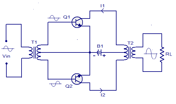
need of a well regulated power supply.The circuit diagram of a classic
Class B push pull amplifier is shown in the diagram below.
The circuit arrangement of the Class B
push pull amplifier is similar to the Class A push pull amplifier except
for the absence of the biasing resistors. T1 is the input coupling
capacitor and the input signal is applied to its primary. Q1 and Q2 are
two identical transistors and their emitter terminals are connected
together. Center tap of the input coupling transformer and the negative
end of the voltage source is connected to the junction point of the
emitter terminals. Positive end of the voltage source is connected to
the center tap of the output coupling transformer. Collector terminals
of each transistor are connected to the respective ends of the primary
of the output coupling transformer T2. Load RL is connected across the
secondary of T2.
The input signal is converted into two
similar but phase opposite signals by the input transformer T1. One out
of these two signals is applied to the base of the upper transistor
while the other one is applied to the base of the other transistor. You
can understand this from the circuit diagram. When transistor Q1 is
driven to the positive side using the positive half of its input signal,
the reverse happens in the transistor Q2. That means when the collector
current of Q1 is going in the increasing direction, the collector
current of Q2 goes in the decreasing direction. Anyway the current flow
through the respective halves of the primary of the T2 will be in same
direction. Have a look at the figure for better understanding. This
current flow through the T2 primary results in a wave form induced
across its secondary. The wave form induced across the secondary is
similar to the original input signal but amplified in terms of
magnitude.
Cross over distortion.
Cross over distortion is a type of
distortion commonly seen in Class B amplifier configurations. As we said
earlier ,the transistor are biased at cut off point in the Class B
amplifier. We all know a Silicon transistor requires 0.7V and a
Germanium diode requires 0.2V of voltage across its base emitter
junction before entering in to conducting mode and this base emitter
voltage is called cut in voltage. Germanium diodes are out of scope in
amplifiers and we can talk about a Class B push pull amplifier based on
Silicon transistors. Since the transistors are biased to cut off, the
voltage across their base emitter junction remains zero during the zero
input condition. The only source for the transistors to get the
necessary cut in voltage is the input signal itself and the required
cut in voltage will be looted from the input signal itself. As a result
portions of the input wave form that are below 0.7V (cut in voltage)
will be cancelled and so the corresponding portions will be absent in
the output wave form too. Have a look at the figure below for better
understanding.
Class AB push pull amplifier.
Class AB is another type of push pull
amplifier which is almost similar to that of a Class A push pull
amplifier and the only difference is that the value of biasing resistors
R1 and R2 are so selected that the transistors are biased just at the
cut in voltage (0.7V). This reduces the time for which both transistors
are simultaneously OFF (the time for which input signal is between
(-0.7V and +0.7V) and so the cross over distortion gets reduced. Of the
above said classes Class A has least distortion, then Class AB and then
Class B. Any way Class AB configuration has reduced efficiency and
wastes a reasonable amount of power during zero input condition. Class B
has the highest efficiency (78.5%), then Class B (between 78.5 to
50%) and then Class A (50%) .


No comments:
Post a Comment